What happened
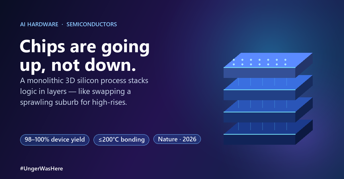
Published in Nature and led by Professor Qing Cao, the work demonstrates true 3D monolithic stacking: layers of 10-nanometer silicon nanomembranes bonded directly on top of each other at 200 degrees Celsius or less, well under the thermal budget that usually fries the layers below. The team stacked three working layers of 625 junctionless transistors each, with 98 to 100 percent yield.
Why this matters: AI's real bottleneck is increasingly distance and power, not just parameter count. Stacking compute vertically shortens the wiring between layers, packs in far denser links, and fits more compute in the same footprint. The team is already working with IBM, Intel, and TSMC, which tells you how seriously the industry takes the vertical path.
It is a research demonstration, not a shipping product. But "low-temperature, high-yield, monolithic 3D" is the exact combination foundries have been chasing for a decade. If you build or buy AI hardware, how much of your roadmap is still betting on going smaller versus going taller?
Source
Reported by Engineers stack transistors into true 3D chips with near-perfect yield via sciencedaily.com, published May 30, 2026.